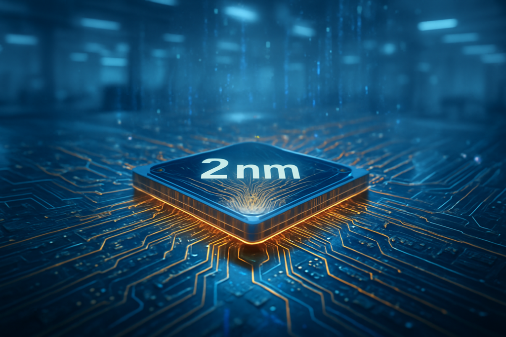
In a move that has sent shockwaves through the global semiconductor industry, Samsung Electronics (KRX: 005930) has officially secured a landmark deal to produce Qualcomm’s (NASDAQ: QCOM) next-generation Snapdragon 8 Gen 5 processors on its cutting-edge 2-nanometer (SF2) production node. Announced during the opening days of CES 2026, the partnership signals a dramatic resurgence for Samsung Foundry, which has spent the better part of the last three years trailing behind the market leader, Taiwan Semiconductor Manufacturing Company (NYSE: TSM). This deal is not merely a supply chain adjustment; it represents a fundamental shift in the competitive landscape of high-end silicon, validating Samsung’s long-term bet on a radical new transistor architecture.
The immediate significance of this announcement cannot be overstated. For Qualcomm, the move to Samsung’s SF2 node for its flagship "Snapdragon 8 Elite Gen 5" (codenamed SM8850s) marks a return to a dual-sourcing strategy designed to mitigate "TSMC risk"—a combination of soaring wafer costs and capacity constraints driven by Apple’s (NASDAQ: AAPL) dominance of TSMC’s 2nm lines. For the broader tech industry, the deal serves as the first major real-world validation of Gate-All-Around (GAA) technology at scale, proving that Samsung has finally overcome the yield hurdles that plagued its earlier 3nm and 4nm efforts.
The Technical Edge: GAA and the Backside Power Advantage
At the heart of Samsung’s resurgence is its proprietary Multi-Bridge Channel FET (MBCFET ) architecture, a specific implementation of Gate-All-Around (GAA) technology. While TSMC is just now transitioning to its first generation of GAA (Nanosheet) with its N2 node, Samsung is already entering its third generation of GAA with the SF2 process. This two-year lead in GAA experience has allowed Samsung to refine the geometry of its nanosheets, enabling wider channels that can be tuned for significantly higher performance or lower power consumption depending on the chip’s requirements.
Technically, the SF2 node offers a staggering 12% increase in performance and a 25% improvement in power efficiency over previous 3nm iterations. However, the true "secret sauce" in the Snapdragon 8 Gen 5 production is Samsung’s early implementation of Backside Power Delivery Network (BSPDN) optimizations. By moving the power rails to the back of the wafer, Samsung has eliminated the "IR drop" (voltage drop) and signal congestion that typically limits clock speeds in high-performance mobile chips. This allows the Snapdragon 8 Gen 5 to maintain peak performance longer without thermal throttling—a critical requirement for the next generation of AI-heavy smartphones.
Initial reactions from the semiconductor research community have been cautiously optimistic. Analysts note that while TSMC still holds a slight lead in absolute transistor density—roughly 235 million transistors per square millimeter compared to Samsung’s 200 million—the gap has narrowed significantly. More importantly, Samsung’s SF2 yields have reportedly stabilized in the 50% to 60% range. While still below TSMC’s gold-standard 80%, this is a massive leap from the sub-20% yields that derailed Samsung’s 3nm launch in 2024, making the SF2 node commercially viable for high-volume flagship devices like the upcoming Galaxy Z Fold 8.
Disrupting the Monopoly: Competitive Implications for Tech Giants
The Samsung-Qualcomm deal creates a new power dynamic in the "foundry wars." For years, TSMC has enjoyed a near-monopoly on the most advanced nodes, allowing it to command premium prices. Reports from late 2025 indicated that TSMC’s 2nm wafers were priced at an eye-watering $30,000 each. Samsung has aggressively countered this by offering its SF2 wafers for approximately $20,000, providing a 33% cost advantage that is irresistible to fabless chipmakers like Qualcomm and potentially NVIDIA (NASDAQ: NVDA).
NVIDIA, in particular, is reportedly watching the Samsung-Qualcomm partnership with intense interest. As TSMC’s capacity remains bottlenecked by Apple and the insatiable demand for Blackwell-successor AI GPUs, NVIDIA is rumored to be in active testing with Samsung’s SF2 node for its next generation of consumer-grade GeForce GPUs and specialized AI ASICs. By diversifying its supply chain, NVIDIA could avoid the "Apple tax" and ensure a more stable supply of silicon for the burgeoning AI PC market.
Meanwhile, for Apple, Samsung’s resurgence acts as a necessary "price ceiling." Even if Apple remains an exclusive TSMC customer for its A20 and M6 chips, the existence of a viable 2nm alternative at Samsung prevents TSMC from exerting absolute pricing power. This competitive pressure is expected to accelerate the roadmap for all players, forcing TSMC to expedite its own 1.6nm (A16) node to maintain its lead.
The Era of Agentic AI and Sovereign Foundries
The broader significance of Samsung’s 2nm success lies in its alignment with two major trends: the rise of "Agentic AI" and the push for "sovereign" semiconductor manufacturing. The Snapdragon 8 Gen 5 is engineered specifically for agentic AI—autonomous AI agents that can navigate apps and perform tasks on a user’s behalf. This requires massive on-device processing power; the SF2-produced chip reportedly delivers a 113% boost in Generative AI processing and can handle 220 tokens per second for on-device Large Language Models (LLMs).
Furthermore, Samsung’s pivot of its $44 billion Taylor, Texas, facility to prioritize 2nm production has significant geopolitical implications. By producing Qualcomm’s flagship chips on U.S. soil, Samsung is positioning itself as a "sovereign foundry" for American tech giants. This move aligns with the goals of the CHIPS Act and provides a strategic alternative to Taiwan-based manufacturing, which remains a point of concern for some Western policymakers and corporate boards.
Comparatively, this milestone is being likened to the "45nm era" of the late 2000s, when the industry last saw a major shift in transistor materials (High-K Metal Gate). The transition to GAA is a similarly fundamental change, and Samsung’s ability to execute on it first gives them a psychological and technical edge that could define the next decade of mobile and AI computing.
Looking Ahead: The Road to 1.4nm and Beyond
As Samsung Foundry regains its footing, the focus is already shifting toward the 1.4nm (SF1.4) node, scheduled for mass production in 2026. Experts predict that the lessons learned from the 2nm SF2 node—particularly regarding GAA nanosheet stability and Backside Power Delivery—will be the foundation for Samsung’s next decade of growth. The company is also heavily investing in 3D IC packaging technologies, which will allow for the vertical stacking of logic and memory, further boosting AI performance.
However, challenges remain. Samsung must continue to improve its yield rates to match TSMC’s efficiency, and it must prove that its SF2 chips can maintain long-term reliability in the field. The upcoming launch of the Galaxy S26 and Z Fold 8 series will be the ultimate "litmus test" for the Snapdragon 8 Gen 5. If these devices deliver on their performance and battery life promises without the overheating issues of the past, Samsung may well reclaim its title as a co-leader in the semiconductor world.
A New Chapter in Silicon History
The deal between Samsung and Qualcomm for 2nm production is a watershed moment that officially ends the era of TSMC’s uncontested dominance at the bleeding edge. By successfully iterating on its GAA architecture and offering a compelling price-to-performance ratio, Samsung has re-established itself as a top-tier foundry capable of supporting the world’s most demanding AI applications.
Key takeaways from this development include the validation of MBCFET technology, the strategic importance of U.S.-based manufacturing in Texas, and the arrival of highly efficient, on-device agentic AI. As we move through 2026, the industry will be watching closely to see if other giants like NVIDIA or even Intel (NASDAQ: INTC) follow Qualcomm’s lead. For now, the "foundry wars" have entered a new, more balanced chapter, promising faster innovation and more competitive pricing for the entire AI ecosystem.
This content is intended for informational purposes only and represents analysis of current AI developments.
TokenRing AI delivers enterprise-grade solutions for multi-agent AI workflow orchestration, AI-powered development tools, and seamless remote collaboration platforms.
For more information, visit https://www.tokenring.ai/.